|
|
Semiconductor & Packaging Industry
TRI provides industry-leading AI-Powered Inspection and Metrology solutions for Semiconductor Front-end to Back-end processes. TRI platforms utilize advanced imaging technologies to detect minuscule and hidden defects, ensuring high-reliability inspection.
Features

AI-Powered Solutions

Interworking with EFEM

Inking Rejection Module

Micro Measurements

High Resolution

Data Traceability

Die/Wire Bonding

Comm. Standard
Multiple Imaging Technologies
-
Digital Fringe Pattern
-
3D Laser for Special Surfaces
-
Depth From Focus (DFF)
-
Short Wave Infrared
-
Confocal Chromatic Sensor
-
X-ray Imaging
Semiconductor Inspection & Metrology Applications
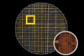
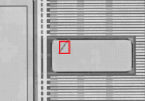
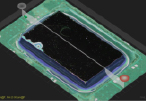
TRI provides precise inspection solutions for Wafer Level & Panel Level Packaging (WLP/PLP), including patterned wafers, bumps, thin film thickness, and TSV. TRI solutions also excel at die bonding and assembly, detecting a wide range of defects, including chipping, cracks, and contamination.
-
Chiplet & Chip-on-Wafer (CoW)
-
System-in-Package (SIP)
-
Advanced WLP
-
TSV Metrology / TGV Inspection
-
µBump & Cu Pillar
-
IR Inner Defects
-
Surface Topology & Profiling
-
Thin Film Thickness
-
Wafer Thickness
-
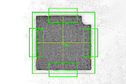
Patterned Wafer
-
After Sawing Defects
-
Die Underfill
-
Glue, Epoxy & Flux
-
Wafer Bumping
-
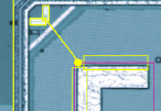
Wire / Die Bonding
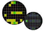
Patterned Wafer
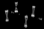
Wire Inspection
Bond Inspection
IR Chipping
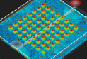
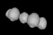
Bump
Mini LED Solder
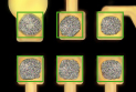
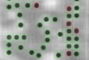
AI-Powered Detection
TRI's AI-powered Inspection is designed to detect
wafer surfaces irregularities, cosmetic defects, foreign
material, and other low-contrast defects.
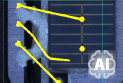
AI Wire Detection
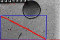
AI Crack Detection
ADVANCED WLP/PLP
TRI's Advanced WLP/PLP inspection and metrology solutions offer high-resolution wafer inspection and high-precision microscopic measurements. TRI provides versatile surface inspection for highly reflective surfaces, wafer bumping, wafer frames, and trenches, alongside ultra-high-speed thin film thickness. and TSV interposer measurement for accurate depth and diameter assessment.
Wafer AVI
Chiplet Metrology
Laser Saw on Wafer
Epoxy / Resin
Sampling
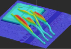
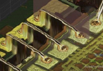
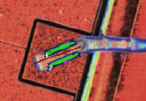
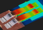
BACK-END Inspection
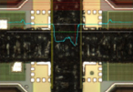
TRI provides advanced inspection and metrology for back-end processes, covering die bonding, wire bonding (down to 15 μm in diameter), and encapsulation (glue / underfill). Key features include Magazine Loader/Unloader, Rejection Module, and more.
IGBT Power Module
0.6 mil Au Wire
Bonding Area
Die Bonding
Ribbon Bond
Metrology Inspection
Easily create formulas with dimensional measurements, inspection parameters, and real measurement values to achieve more precise inspection with less false calls and lower escape.
|
METROLOGY APPLICATIONS |
|
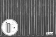
Through-Silicon Via (TSV) |
Spot Size: 50 µm, 25 µm
TSV aspect ratio: Max 30:1
Via diameter: 3-20 µm |
|
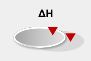
Thin Film Thickness |
Film Thickness Range:
100 nm to 30 µm
Measurable Film Types:
SiO2, PI, PR, SIN
Measurable Substrates: Si, Glass |
|
Other Applications |
Chiplet Measurements,
Wafer Thickness |
Wafer Chip
Thin Film Thickness
TSV Metrology
Wafer Thickness
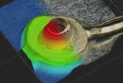
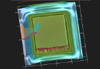
X-Ray Inspection
TRI's SEMI AXI solutions meet OSAT requirements with faster cycle times and sharper images. The AI-Powered X-ray solutions are capable of identifying defects as small as 14 x 14 μm and ensure high reliability of GR&R < 10%. The SEMI AXI also support SECS/GEM and have optional vacuum block to ensures stability for accurate detection.
Cu Pillar
C4 Bump
3D CT Bump
TGV Void Detection
|

